Semiconductor heterostructures
Semiconductor materials, heterostructure, and integration
Semiconductor heterostructures, consisting of different materials and their integration, play a crucial role in the development of multifunctional and high-performance semiconductor devices. We study the following topics in this area:
Current topics:
- Monolithic integration of ultrawide-bandgap semiconductor film and silicon substrate
- Fabrication process for mechanically flexible high-quality semiconductor devices
- Semiconductor heterostructures with efficient thermal management
Past topics:
- Single-crystalline semiconductor films on flexible metal tapes
- New epitaxy of piezoelectric thin films
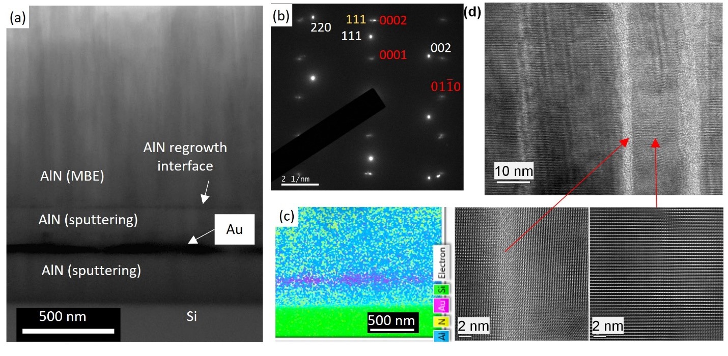 |
Crack-free single-crystalline AlN on Si substrate: (a) Cross-sectional STEM bright-field image; (b) overlapped SADP of Au and AlN; (c) EDS map of cross section; and (d) high-resolution image showing columns and column boundaries. (adapted from doi: 10.1063/5.0219833) |
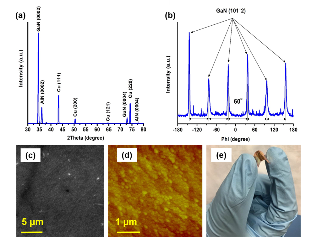 |
Single-crystalline GaN and AlN films on polycrystalline Cu tape using 2D materials: (a) XRD 2θ-ω scan of GaN on AlN/graphene/Cu foil; (b) XRD φ scan of GaN {102} peaks; (c) SEM and (d) AFM images for a GaN film; (e) photo of a flexible GaN substrate. (adapted from doi: 10.1039/d0tc04634e) |